Samsung S7 Circuit Diagram
S8 samsung g950f schematic sm board تشريح بورد [get 30+] galaxy s6 schematic diagram download Solved: diagram for samsung galaxy s7 edge (g935f)
[Get 30+] Galaxy S6 Schematic Diagram Download
S8 g955f schematics Samsung schematic diagrama 6s схема g920f wiring schematics инструкция angelux s5 duos Schematic g935f sm
Teardown ifixit s7
Samsung galaxy s8 plus sm-g955f schematicsS7 diagram edge samsung galaxy Samsung galaxy s7 edge sm-g935f schematic diagram service manualSamsung schematic s8 layout pdf schematics components diagrams manual.
[get 29+] galaxy s6 schematic diagram downloadSamsung galaxy s7 edge (g935a) diagram [get 30+] galaxy s6 schematic diagram downloadSamsung galaxy s7 teardown.

Samsung s8 sm-g950f board schematic
Samsung s8 schematic pdfPhone pcb diagram mobile samsung parts smartphone galaxy part motherboard board s7 components sm phones schematic layout circuit iphone flash S7 schematics g935fMobile phone pcb diagram with part.
S6 schematics g925 .
![[Get 30+] Galaxy S6 Schematic Diagram Download](https://i2.wp.com/appleunlockstore.com/images/gallery/Manuals/G920F.jpg)
![[Get 29+] Galaxy S6 Schematic Diagram Download](https://i2.wp.com/phonelumi.com/wp-content/uploads/2016/09/schematics-samsung-s7edge.jpg)
[Get 29+] Galaxy S6 Schematic Diagram Download
![[Get 30+] Galaxy S6 Schematic Diagram Download](https://i2.wp.com/phonelumi.com/wp-content/uploads/2016/10/samsung-s6-edge-schematics.png?x45285)
[Get 30+] Galaxy S6 Schematic Diagram Download

Samsung Galaxy S8 Plus SM-G955F schematics

Samsung S8 Schematic PDF - Schematic Diagram

Mobile Phone PCB Diagram With Part | Mobile Repairing Online

Samsung Galaxy S7 edge (G935A) Diagram - AT&T Device Support
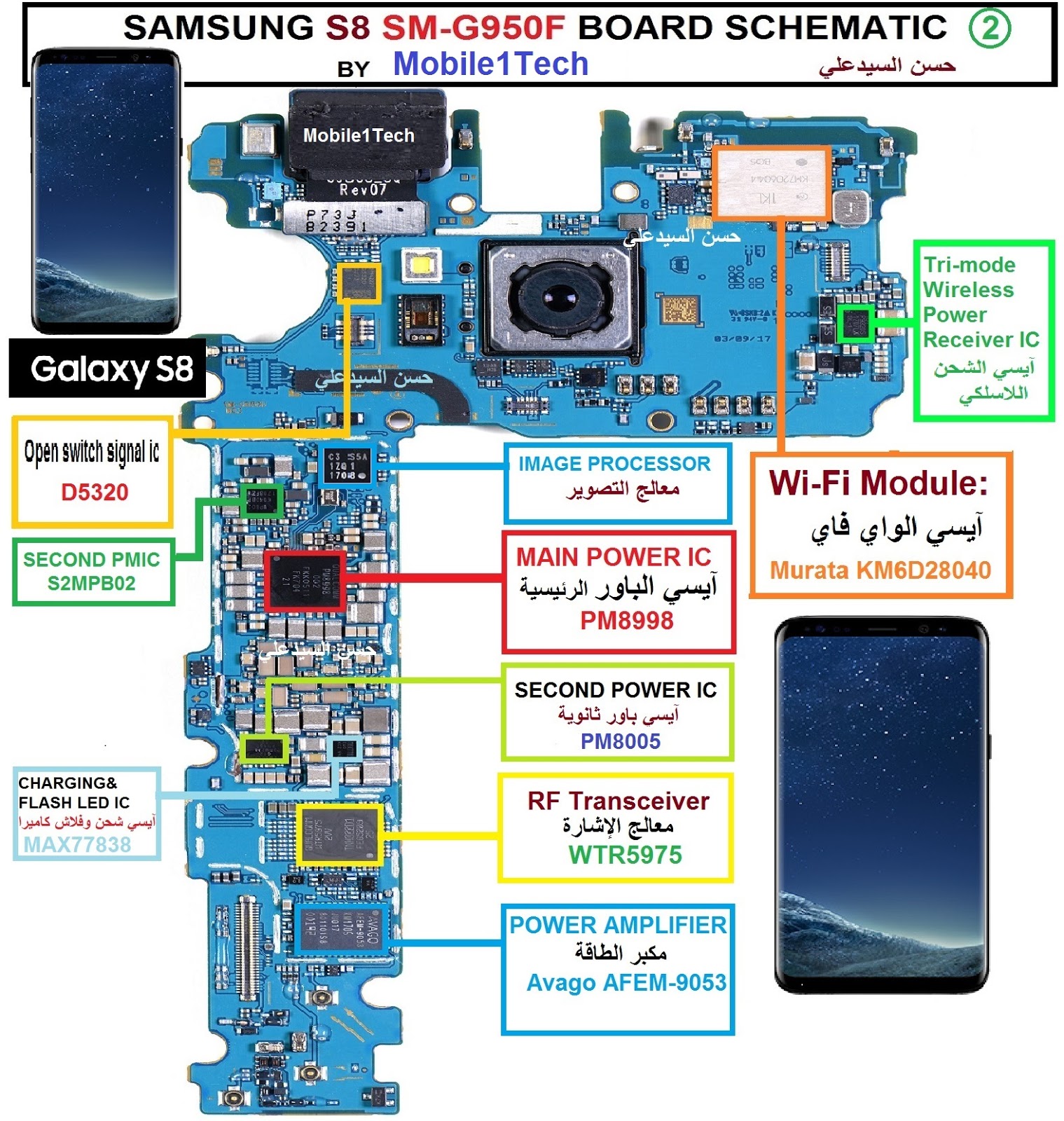
SAMSUNG S8 SM-G950F BOARD SCHEMATIC

SAMSUNG GALAXY S7 EDGE SM-G935F SCHEMATIC DIAGRAM Service Manual

Samsung Galaxy S7 Teardown - iFixit
